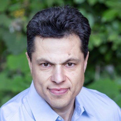
Dr. Leonid, as a Dielectric Etch Staff Process Engineer at Lam Research, is at the forefront of advancing semiconductor manufacturing technologies, particularly in the realm of dielectric dry etching. His expertise is pivotal in the research and development of innovative etch processes tailored for the...
Dr. Leonid, as a Dielectric Etch Staff Process Engineer at Lam Research, is at the forefront of advancing semiconductor manufacturing technologies, particularly in the realm of dielectric dry etching. His expertise is pivotal in the research and development of innovative etch processes tailored for the most demanding applications in DRAM and 3D NAND Flash memory. With a focus on high-performance solutions, Dr. Leonid leads initiatives that encompass the etching of 3D and 2D NAND Flash memory contacts, DRAM capacitor cell etching, and the development of high aspect ratio contacts (HARC).
His role involves not only the enhancement of existing processes but also the innovation of new chemical solutions and hardware development, ensuring that Lam Research maintains its technological and market share dominance in the semiconductor industry. Dr. Leonid's work on carbon and poly-silicon mask development is particularly noteworthy, as it addresses the challenges posed by the increasing complexity of modern chip architectures.
Leveraging his extensive skills in plasma etching, spectroscopy, and metrology, Dr. Leonid employs advanced characterization techniques, including X-ray photoelectron spectroscopy (XPS) and various microscopy methods, to analyze and refine etch processes. His contributions to molecular layer deposition and nanotechnology further solidify his reputation as a leader in the field. As the semiconductor landscape continues to evolve, Dr. Leonid's commitment to innovation and excellence positions him as a key player in driving the future of memory technology, ensuring that Lam Research remains at the cutting edge of the industry.


